A significant technological boost has transformed industries around the world. Thermal imaging lenses are used by the semiconductor industry to their fullest potential.
Semiconductor Chip Production
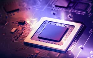
Semiconductor chip is a main component of computers, mobile phones, automobiles, and appliances. Photolithography is used by manufacturers to make them. This involves shining light from a mask through a wafer that has been coated with a material sensitive to light. The exposure to light alters the material’s characteristics, which allows the etching patterns on the wafer surface.
Ultraviolet Lenses & Semiconductors
Ultraviolet Lenses Types Used in Semiconductor Manufacturing
In photolithography, Ultraviolet Lenses are used to focus light onto the wafer. These lenses are made of materials such as calcium fluoride or quartz that allows UV light to pass. There are many types of UV lenses including Fresnel and refractive lenses.
Quartz is a common material for making lenses. The lenses bend the light when it passes through them. Fresnel lens are made up of several curved surfaces. They focus the light onto the wafer by re-directing it.
Both scanning and projection photolithography systems come with Ultraviolet Lenses. In scanning photolithography, the mask is directly in front of the UV light. The wafer is focused by the lens after the light passes through the mask.
Ultraviolet Lenses use different materials
Quartz, calcium fluoride and magnesium are among the materials used to make UV lenses. Each material is unique and has different properties that make it suitable for various applications. Quartz lenses, for example, are used to project light with greater accuracy onto wafers in high-end systems. This is because quartz lenses have a very high index of reflection.
Fluoride Calcium
In scanning systems, calcium fluoride lens are used because they have lower refraction index and therefore less likely to produce diffraction effects. Magnesium fluoride lenses, which have a high transmittance rate, are used both in scanning and projection systems. This allows more light to reach wafers.
The semiconductor industry is constantly evolving, and there are new manufacturing processes being developed. Ultraviolet Lenses are essential to these processes and will continue to be used more.
Ultraviolet Lenses excel at quality monitoring and inspection
Precision is required in semiconductor fabrication. Quality control is essential to the manufacturing process because any mistake can lead to a failure of a semiconductor chip. UV lenses can detect tiny flaws early on in the production process.
Inspection of parts at high speed reduces manufacturing defects.
In the past, machine-vision lens have worked in the visible spectrum. This allowed captured images to reflect what humans see. LEDs have been used in non-UV applications, but the high resolution users can achieve in the visible spectrum has led to the development of lenses which function in the UV area of the electromagnetic spectrum.
Improves accuracy with Detailed Resolution
This is because UV wavelengths are shorter than visible wavelengths, and can detect more detail in objects. This makes them more useful in semiconductor manufacturing as it allows companies to quickly check for errors and monitor production processes.
Defect Review Systems Continue To Speed Up
As chips get smaller, the inspection process is centered on shorter wavelength light. The smaller the chips, the more defects there are. This requires even more precision in cameras and lenses.
New systems are being developed by manufacturers that use defect-review imaging tools, wafer inspection tools, and reticle inspection tools. New designs employ cameras and optics that operate in the deep-UV range of 150nm to300nm.
In the same way that semiconductors are being manufactured, UV technology is also used to make UV Lens. The result is that products get smaller and faster. This allows for more advancements.
Ultraviolet Lenses are indispensable for product inspection. They eliminate bottlenecks caused by less automated methods of checking every unit for error-free. They continue to improve their core functions, and will continue playing a vital role in detecting quality issues.
New Innovations on the Horizon
Companies that fabricate chips will need Ultraviolet Lenses to stay competitive. There are many breakthroughs in extreme ultraviolet (EUV) Photolithography.
These advancements continue to unlock new applications, which assist semiconductor manufacturers in their core mission. If you look at the headlines of recent years, it is clear that EUV technology has continued to break through barriers with remarkable speed.
EUV will help semiconductor manufacturers meet the growing demand.


